BUSINESS
QUALITY
It will explain problems and solutions of nano contaminants recovery technology in Silicon Wafer and Semiconductor industries.
Conventional Problems
Procedures to collect nano contaminants of sides of wafers
- Stand the wafers vertically
- Dip only the edges of wafers in the liquid while rotating
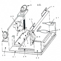
11-204604
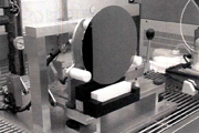
C.Sparks et. Al., Proceedings of SPINE vol.5041(2003)pp.99.
Problems
- A specific device to rotate wafers vertically is required.
- Since wafers are dipped, the amount of liquid for storing cannot be reduced.
NAS Giken developed an innovative Device
No need to place a wafer vertically, but horizontally as conventionally
The amount of liquid used when sampling can be less than before
Solutions by NAS Giken
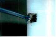
Produced Liquid Holders for Bevel Recovery Utilizing Surface Tension
- Bevel part of the wafer is dipped with the liquid that is squeezed out from the side slit of the liquid holder.
- Because of surface tension, the liquid does not flow out the side part of the liquid holder.
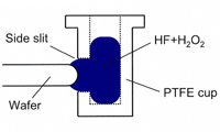
Process of Bevel Recovery
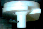
- Rotate wafers to dip only the bevel part of wafer into the liquid.
- By adjusting the position of the wafer, it can be set so that the liquid does not spread into the front and back surfaces of the wafer.
AFTER-SALES SERVICE
The service for NAS Giken tools guarantees your complete satisfaction. Please feel free to ask if you have any enquiries concerning our devices.
Perfect After-Sales Service
We provide maintenance service not all over Japan also overseas customers.
Our sales support shall respond to customer inquiries from Japan in within 24 hours (from overseas less than 48 hours).
When confirming maintenance details, we hold online meetings with as appropriate.
CONTACT US
Please complete the form and submit if you request a quote or product information.
A NAS Giken representative will contact you regarding your request.
Call to speak to us 9:00-17:00
(Monday to Friday)
Tel. +81-42-557-5207
![]()
Inquiry Form

